- 您现在的位置:买卖IC网 > Sheet目录2004 > LTC1482CMS8 (Linear Technology)IC TXRX RS485 LOWPWR 8-MSOP
2
LTC1482
ABSOLUTE MAXIMUM RATINGS
W
WW
U
(Note 1)
Supply Voltage (VCC)............................................... 6.5V
Control Input Voltages ................. – 0.3V to (VCC + 0.3V)
Carrier Detect Voltage ................................. – 0.3V to 8V
Driver Input Voltage ..................... – 0.3V to (VCC + 0.3V)
Driver Output Voltages ................................. – 7V to 10V
Receiver Input Voltages (Driver Disabled) .. –12V to 14V
Receiver Output Voltage ............... – 0.3V to (VCC + 0.3V)
Junction Temperature .......................................... 125
°C
Operating Temperature Range
LTC1482C ........................................ 0
°C ≤ TA ≤ 70°C
LTC1482I ...................................... – 40
°C ≤ TA ≤ 85°C
Storage Temperature Range .................. – 65
°C to 150°C
Lead Temperature (Soldering, 10 sec)................... 300
°C
SYMBOL
PARAMETER
CONDITIONS
MIN
TYP
MAX
UNITS
VOD1
Differential Driver Output Voltage (Unloaded)
IOUT = 0
q
VCC
V
VOD2
Differential Driver Output Voltage (with Load)
R = 50
(RS422)
q
2V
R = 27
(RS485) Figure 1
q
1.5
5
V
R = 22
, Figure 1
q
1.5
5
V
VOD3
Differential Driver Output Voltage
VTST = – 7V to 12V, Figure 2
q
1.5
5
V
(with Common Mode)
VOD
Change in Magnitude of Driver Differential
R = 22
, 27 or R = 50, Figure 1
q
0.2
V
Output Voltage for Complementary Output States
VTST = – 7V to 12V, Figure 2
VOC
Driver Common Mode Output Voltage
R = 22
, 27 or R = 50, Figure 1
q
3V
|VOC|
Change in Magnitude of Driver Common Mode
R = 22
, 27 or R = 50, Figure 1
q
0.2
V
Output Voltage for Complementary Output States
VIH
Input High Voltage
DE, DI/SHDN
q
2V
VIL
Input Low Voltage
DE, DI/SHDN
q
0.8
V
IIN1
Input Current
DE, DI/SHDN
q
±2
A
IIN2
Input Current (A, B) with Driver Disabled
DE = 0, VCC = 0 or 5V, VIN = 12V
q
1.0
mA
DE = 0, VCC = 0 or 5V, VIN = –7V
q
– 0.8
mA
VTHRO
Differential Input Threshold Voltage for Receiver
– 7V
≤ VCM ≤ 12V, DE = 0
q
– 0.20
– 0.015
V
ELECTRICAL CHARACTERISTICS The q denotes the specifications which apply over the full operating
temperature range, otherwise specifications are at TA = 25°C. VCC = 5V ±5% (Notes 2 and 3) unless otherwise noted.
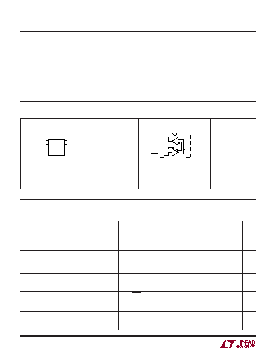
PACKAGE/ORDER INFORMATION
W
U
ORDER PART
NUMBER
ORDER PART
NUMBER
LTC1482CMS8
LTC1482CN8
LTC1482CS8
LTC1482IN8
LTC1482IS8
S8 PART MARKING
1482
1482I
MS8 PART MARKING
LTCB
TJMAX = 125°C, θJA = 200°C/ W
1
2
3
4
RO
CD
DE
DI/SHDN
8
7
6
5
VCC
B
A
GND
TOP VIEW
MS8 PACKAGE
8-LEAD PLASTIC MSOP
TJMAX = 125°C, θJA = 130°C/ W (N8)
TJMAX = 125°C, θJA = 135°C/ W (S8)
1
2
3
4
8
7
6
5
TOP VIEW
RO
CD
DE
DI/SHDN
VCC
B
A
GND
N8 PACKAGE
8-LEAD PDIP
S8 PACKAGE
8-LEAD PLASTIC SO
Consult factory for Military grade parts.
发布紧急采购,3分钟左右您将得到回复。
相关PDF资料
LTC1484IS8#TRPBF
IC TXRX RS485 LOWPWR 8-SOIC
LTC1518IS#TRPBF
IC LINE RCVR RS485 QUAD 16-SOIC
LTC1543IG#TRPBF
IC TXRX SOFTWARE SELECTBL 28SSOP
LTC1544IG#TRPBF
IC TXRX SOFTWARE SELECTBL 28SSOP
LTC1545CG
IC TXRX SOFTWARE SELECTBL 36SSOP
LTC1590IS#TRPBF
IC D/A CONV 12BIT DUAL 16-SOIC
LTC1592AIG#TRPBF
IC D/A CONV 16BIT SOFTSPAN16SSOP
LTC1595AIN8
IC D/A CONV 16BIT MULTPLYNG 8DIP
相关代理商/技术参数
LTC1482CMS8#PBF
功能描述:IC TXRX RS485 LOWPWR 8-MSOP RoHS:是 类别:集成电路 (IC) >> 接口 - 驱动器,接收器,收发器 系列:- 标准包装:1 系列:- 类型:线路收发器 驱动器/接收器数:5/3 规程:RS232 电源电压:3 V ~ 5.5 V 安装类型:表面贴装 封装/外壳:28-SOIC(0.295",7.50mm 宽) 供应商设备封装:28-SOIC 包装:Digi-Reel® 产品目录页面:918 (CN2011-ZH PDF) 其它名称:296-25096-6
LTC1482CMS8#TR
功能描述:IC TXRX RS485 DET/FAILSAFE 8MSOP RoHS:否 类别:集成电路 (IC) >> 接口 - 驱动器,接收器,收发器 系列:- 标准包装:27 系列:- 类型:收发器 驱动器/接收器数:3/3 规程:RS232,RS485 电源电压:4.75 V ~ 5.25 V 安装类型:表面贴装 封装/外壳:28-SOIC(0.295",7.50mm 宽) 供应商设备封装:28-SOIC 包装:管件
LTC1482CMS8#TRPBF
功能描述:IC TXRX RS485 LOWPWR 8-MSOP RoHS:是 类别:集成电路 (IC) >> 接口 - 驱动器,接收器,收发器 系列:- 标准包装:27 系列:- 类型:收发器 驱动器/接收器数:3/3 规程:RS232,RS485 电源电压:4.75 V ~ 5.25 V 安装类型:表面贴装 封装/外壳:28-SOIC(0.295",7.50mm 宽) 供应商设备封装:28-SOIC 包装:管件
LTC1482CN8
功能描述:IC TXRX RS485 LOWPWR 8-DIP RoHS:否 类别:集成电路 (IC) >> 接口 - 驱动器,接收器,收发器 系列:- 标准包装:1 系列:- 类型:线路收发器 驱动器/接收器数:5/3 规程:RS232 电源电压:3 V ~ 5.5 V 安装类型:表面贴装 封装/外壳:28-SOIC(0.295",7.50mm 宽) 供应商设备封装:28-SOIC 包装:Digi-Reel® 产品目录页面:918 (CN2011-ZH PDF) 其它名称:296-25096-6
LTC1482CN8#PBF
功能描述:IC TXRX RS485 LOWPWR 8-DIP RoHS:是 类别:集成电路 (IC) >> 接口 - 驱动器,接收器,收发器 系列:- 标准包装:1 系列:- 类型:线路收发器 驱动器/接收器数:5/3 规程:RS232 电源电压:3 V ~ 5.5 V 安装类型:表面贴装 封装/外壳:28-SOIC(0.295",7.50mm 宽) 供应商设备封装:28-SOIC 包装:Digi-Reel® 产品目录页面:918 (CN2011-ZH PDF) 其它名称:296-25096-6
LTC1482CS8
功能描述:IC TXRX RS485 LOWPWR 8-SOIC RoHS:否 类别:集成电路 (IC) >> 接口 - 驱动器,接收器,收发器 系列:- 标准包装:121 系列:- 类型:收发器 驱动器/接收器数:1/1 规程:RS422,RS485 电源电压:3 V ~ 3.6 V 安装类型:表面贴装 封装/外壳:10-WFDFN 裸露焊盘 供应商设备封装:10-DFN(3x3) 包装:管件
LTC1482CS8#PBF
功能描述:IC TXRX RS485 LOWPWR 8-SOIC RoHS:是 类别:集成电路 (IC) >> 接口 - 驱动器,接收器,收发器 系列:- 产品培训模块:RS-232 & USB Transceiver 标准包装:2,000 系列:- 类型:收发器 驱动器/接收器数:1/1 规程:RS232 电源电压:3 V ~ 5.5 V 安装类型:表面贴装 封装/外壳:16-SSOP(0.209",5.30mm 宽) 供应商设备封装:16-SSOP 包装:带卷 (TR) 其它名称:296-19849-2
LTC1482CS8#PBF
制造商:Linear Technology 功能描述:RS485 Driver IC